Electrical properties of ScN(111) layers grown on semi-insulating GaN(0001) by plasma-assisted molecular beam epitaxy
After more than half a century of research, understanding electron scattering mechanisms in scandium nitride (ScN) has remained a significant challenge, primarily due to high impurity concentrations in scandium sources. In a groundbreaking study published in Phys. Rev. Appl. 22, 014067 (2024), researchers at PDI overcame this long-standing limitation by growing high-purity ScN(111) layers on nearly lattice-matched semi-insulating GaN(0001) using plasma-assisted molecular beam epitaxy. By employing an ultra-high-purity Sc source, the researchers drastically reduced impurity levels, enabling an unprecedented examination of ScN’s intrinsic electrical properties. Crucially, the nearly lattice-matched ScN/GaN hetero-interface minimizes structural defects, leading to significantly higher mobility than ScN grown on other substrates. For the first time, nondegenerate ScN was realized—a major breakthrough in semiconductor research. This pivotal achievement provides invaluable insights into electron scattering mechanisms and addresses long-standing challenges associated with impurity-induced effects in ScN.
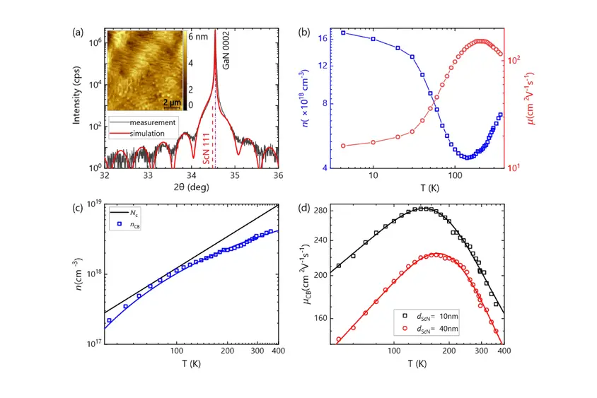
Through temperature-dependent Hall-effect measurements, the study reveals electron concentrations of 0.7–3.1 × 10¹⁹ cm⁻³ and mobilities reaching 160 cm²V⁻¹s⁻¹ at room temperature, with a remarkable peak mobility of 280 cm²V⁻¹s⁻¹ in the 140–180 K range for the 10-nm-thick layer. By deeply investigating the conductivity, researchers found that the conduction in the layers follows a two-band model, involving both an impurity band and the conduction band. Electron mobility is primarily limited by ionized-impurity scattering at low temperatures and optical phonon scattering at higher temperatures.
These findings establish ScN as a highly promising material for next-generation electronic and optoelectronic devices. Its combination of high electron mobility and seamless integration with GaN paves the way for energy-efficient transistors, advanced thermoelectric materials for energy harvesting, and high-performance integrated device architectures. By bridging fundamental materials research with cutting-edge technology, this work lays the foundation for transformative applications in high-performance transistors, optoelectronics, energy harvesting, and next-generation semiconductor technologies. It further strengthens transition-metal nitrides as key materials in future device engineering.

Title: Electrical properties of ScN(111) layers grown on semi-insulating GaN(0001) by plasma-assisted molecular beam epitaxy
Authors: D. V. Dinh, O. Brandt
Source: Phys. Rev. Appl., 22, 014067 (2024)
DOI: 10.1103/PhysRevApplied.22.014067