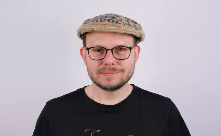
Dr. Jonas Lähnemann
Senior Scientist

Forschungsschwerpunkte
Projekte
Kompetenzen
Responsible scientist for analytical scanning electron microscopy and the Application Laboratory Time-Resolved Cathodoluminescence Spectroscopy. Collaborating with many internal and external partners, Jonas has worked on a broad range of materials spanning from AlN, GaN and hBN for UV applications, over (In,Ga)N and Ga(P,N) in the visible spectral range to (In,Ga)As and In(As,Sb) in the near infrared. He has collected extensive experience in correlating different spatially-resolved techniques, in particular on semiconductor nanowires. Notable work also includes the role of extended defects, such as stacking faults and dislocations, in GaN and carrier diffusion in this material system.