Challenges in the growth of Indium Selenide Films for Advanced Optoelectronic applications
/ Announcements
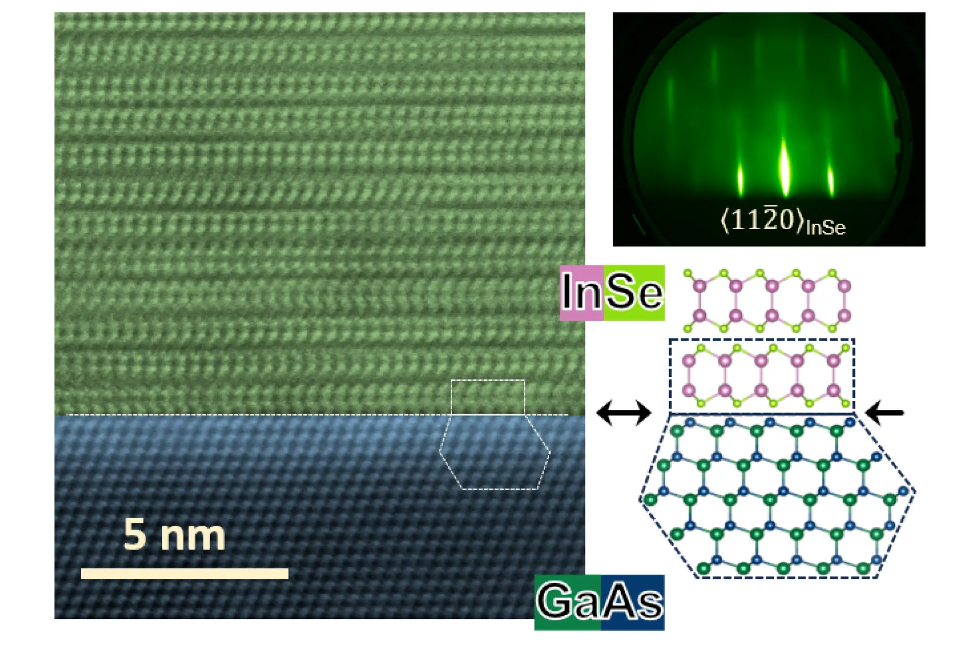
A collaborative research effort by scientists from the Paul-Drude-Institut für Festkörperelektronik (PDI) in Berlin, the Pennsylvania State University, and the New Jersey Institute of Technology has demonstrated the successful growth of high-quality indium selenide (InSe) thin films on semi-insulating gallium arsenide GaAs(111)B substrates using molecular beam epitaxy (MBE). This result addresses a very timely challenge in synthesizing InSe with controlled crystalline quality and integrating it with a compound semiconductor platform, thus opening up new possibilities for high-performance optoelectronic devices, including photodetectors and solar cells.
Indium selenide is a layered van der Waals semiconductor with promising characteristics for next-generation electronics and photonics. Specifically, the high carrier mobility at room temperature renders it very suitable for electronic applications. A reliable bottom-up synthesis approach of these materials that allows for epitaxial integration with established compound semiconductor platforms has been so far elusive. In particular the question arises, if under thin film growth conditions available in molecular beam epitaxy the formation of single-phase InSe can be achieved.
The research team reported that GaAs(111)B indeed served as an ideal substrate for InSe epitaxy, providing a favorable nucleation environment. Careful analysis using X-ray diffraction and Raman spectroscopy revealed that despite the excellent control over growth conditions different polytypes may have formed during growth and were present in the film. While the targeted g-InSe was the dominant polytype, slight lateral shifts of adjacent layers separated by the van der Waals gap in the InSe films gave rise to the formation of additional polytypes. Detailed microstructure analysis using scanning transmission electron microscopy revealed that although InSe nucleates Se-first on GaAs(111)B surfaces – unlike in the case of Si(111) where In forms a direct bond with Si – the polytype domain arrangement can be found down to the nanometer scale and contained both centrosymmetric and non-centrosymmetric polytypes. In addition, the detailed analysis revealed for the first time the presence of the so-called ‘S’-type polymorph, a theoretically predicted configuration with a 12.9 meV per formula unit higher energy compared to the conventional ‘C’-type polymorph. A systematic energetics analysis by density functional theory was performed for the different polytypes and polymorphs that were experimentally observed. Their formation energies are found to be very similar in density functional theory. Similarly, energy differences between different stacking sequences were small and well within the thermal budget of the growth temperature employed. Their differences in electronic band structure gave rise to an energetic disorder at the nanoscale, explaining the suppression of electronic transport at room temperature due to the presence of significant energy barriers emerging at polytype /polymorph domain boundaries in the film that dominated the macroscopic electronic transport characteristics in the films.
While the combined experimental/theoretical study unveiled a set of challenges in the bottom-up synthesis approach of these van der Waals compounds, it also holds promise not only to experimentally realize energetically less favorable polytypes that intrinsically lack inversion symmetry even in the single layer limit, but also offers the potential to grow layered chalcogenide heterostructures with controlled conduction- and valence band offsets, if the control of polytype and polymorph formation becomes accessible using bottom-up synthesis approaches – like molecular beam epitaxy. As many highly sought-after 2D materials present in a similar polytype and polymorph abundance, the results of this study have far-reaching implications for the general synthesis of such 2D materials. While an improved understanding and control over growth conditions is necessary to stabilize the layer polymorph of choice and to suppress the nanoscale polytype domain formation, the ability to inscribe a specific layer sequence on demand utilizing the layer-by-layer growth mode available in MBE is a suitable route towards engineering functional stacks of specific polytypes in 2D materials, offering superior electronic properties over their centrosymmetric counterparts and epitaxially integrating them with non-centrosymmetric polytypes in a controlled fashion.
Title: Mixed polytype/polymorph formation in InSe films grown by molecular beam epitaxy on GaAs(111)B
Authors: Maria Hilse, Justin Rodriguez, Jennifer Gray, Jinyuan Yao, Shaoqing Ding, Derrick Shao Heng Liu, Mo Li, Joshua Young, Ying Liu & Roman Engel-Herbert
Source: npj 2D Mater. Appl., 9, 19 (2025)
DOI: 10.1038/s41699-025-00535-7