Grown, Not Stacked: Epitaxial 2D Magnet Heterostructures and Their Unusual Physics
/ Scientific Highlight
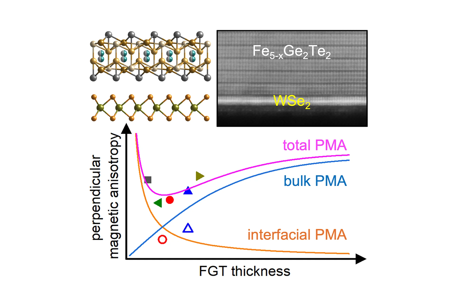
H. Lv et al., Advanced Functional Materials, © Authors, published under CC BY 4.0. DOI: 10.1002/adfm.79018
Two-dimensional magnets only a few atoms thick could enable a new generation of energy-efficient electronics, but building devices from them usually means stacking tiny flakes by hand. A new study led by Hua Lv, João Marcelo J. Lopes and their colleagues at the Paul-Drude-Institut für Festkörperelektronik (PDI), in collaboration with the Pennsylvania State University, Johannes Gutenberg University Mainz, and the Catalan Institute of Nanoscience and Nanotechnology (ICN2) in Barcelona, has instead realized such structures directly by epitaxy, a method crucial for industrial electronics manufacturing. The team also revealed unconventional physics at their interfaces. The results are published in Advanced Functional Materials.
Two-dimensional magnets can keep their magnetic order down to a few atomic layers. When they are combined with semiconducting 2D materials such as transition-metal dichalcogenides to form heterostructures, electrons in one layer feel the presence of the other. These proximity effects offer an efficient way to tune magnetism through the interface. For spintronics, which uses the spin of the electron as well as its charge to store and process information, this opens routes to devices that promise to use much less energy than today's chips.
The obstacle is manufacturing. Most such heterostructures are still made by exfoliating flakes from bulk crystals and stacking them under a microscope. The approach has produced remarkable physics, but it gives limited control over layer thickness and interface quality, and cannot be scaled to wafers.
The PDI team grew the ferromagnet Fe₅₋ₓGeTe₂ (FGT) directly on the semiconductor tungsten diselenide (WSe₂), building complete heterostructures with clean, well-defined interfaces and precisely controlled thickness. The structures are ferromagnetic at room temperature, an important requirement for practical devices. Their magnetisation also points perpendicular to the layers, which is favoured for energy-efficient high-density data storage.
Magnetic and transport measurements revealed temperature-driven magnetic transitions, higher-order contributions to the magnetic anisotropy and a large anisotropic magnetoresistance. These features indicate that the different iron sublattices in FGT contribute to different extents to the magnetic and transport properties.
Several observations did not follow the expected trends. The exchange bias, a shift of the magnetic hysteresis loop, changed sign depending on both layer thickness and temperature. The unconventional Hall effect showed a thickness dependence opposite to the usual one, and the perpendicular anisotropy varied non-monotonically with thickness. The team highlights the role of interfacial effects in these anomalies, which become visible because the epitaxial interfaces are so clean.
The study is fundamental research, but it addresses a practical bottleneck. 2D magnetic heterostructures can only become part of future electronics if they can be made reproducibly and at scale. The results show that FGT/WSe₂ structures can be grown with methods compatible with existing industrial techniques while keeping the interface physics that makes them interesting. This gives a scalable platform both for exploring 2D physics and for developing future 2D spintronic devices.
Title: Proximity-tuned magnetic and transport anomalies in all-epitaxial Fe₅₋ₓGeTe₂/WSe₂ Van der Waals heterostructures
Authors: H. Lv, T. Shinwari, K. Khan, J. Herfort, C. Chen, J. M. Redwing, M. Loyal, G. Jakob, M. Kläui, A. Trampert, B. Mundet, B. Ballesteros, M. Ramsteiner, R. Engel-Herbert, M. Hanke, J. M. J. Lopes
Source: Adv. Funct. Mater. (2026)
DOI: 10.1002/adfm.79018
CReAs: Magnetic Materials for Spintronics and Magnetoacoustics, 2D Materials