Attoseconds at Nanometers
Optical spectroscopy captures ultra-fast events, while electron microscopy reveals ultra-small details. But can a technology bridge both extremes, offering high speed and fine resolution? Join Dr. Kagiso Loeto to discover the research pushing the boundaries of how we see and measure the microscopic world.
In school, we are taught that everything around us is made up of atoms, which are built from electrons and a central nucleus, forming the basic elements seen on the periodic table of elements. These atoms can link together creating the molecules and solid materials we see and use every day. Understanding the behaviours of these atoms, molecules and solids is crucial for scientific and technological advancement.
Why is Attoscience Necessary?
Oftentimes, the atoms, molecules and solids are illustrated with simple diagrams and models. The reality is that we know surprisingly little about how electrons and nuclei move within these systems especially at the small scale. Observing them is a huge challenge because these movements happen on incredibly small scales and within unbelievably short times.
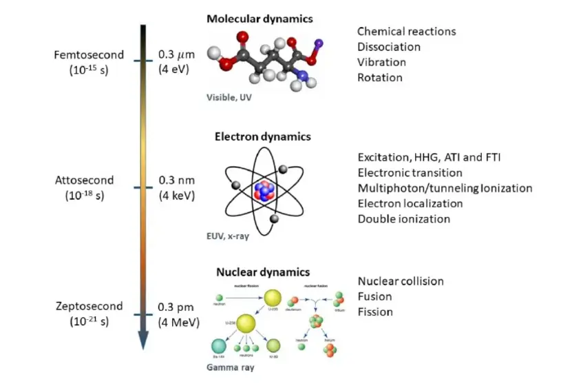
Processes like molecular movement or an electron’s jump between atoms happen in just a few hundred attoseconds (one attosecond is a quintillionth of a second) at the scale of nanometers (one nanometer is a billionth of a meter). Capturing these fleeting actions at such small scales is key to understanding the atomic world. To date, no such instrument exists that can perform both tasks simultaneously. But, by combining knowledge from the fields of attosecond physics, optical spectroscopy and electron microscopy, such an instrument can be achieved.
Challenging the Status Quo
In conventional attosecond physics, scientists use ultra-fast laser pulses produced by a process called high-harmonic generation to observe events on the timescale of attoseconds. While this method provides incredibly fine time resolution, the laser-light is diffraction limited and cannot provide the resolutions required to study nanoscopic details in matter. Electron microscopy, on the other hand, can routinely capture detailed images at the nanoscale but lacks the attosecond time resolution because of limitations in using electron beams. This presents an open challenge for researchers: developing electron microscopes capable of producing attosecond electron pulses, which would combine both nanoscale spatial and attosecond time resolution for a fuller picture of atomic and electronic processes.
Revolutionizing Materials Science and Technology
Achieving attosecond science within an electron microscope would be ground-breaking, we could directly observe electron movements within atoms, molecules, and materials in real-time, offering insights into fundamental processes like electron transfer, bond formation, and breaking at the atomic level. This would provide a much deeper understanding of how electronic properties emerge and evolve. This could lead to the design of more efficient materials for electronics, energy storage, and light-based technologies by understanding their behaviour at unprecedented speeds and scales.
Presented by

Dr. Kagiso Loeto, Semiconductor Microscopy and Spectroscopy
