Love Science, Hate WissZeitVG
Short-term contracts limit scientific careers in Germany, with the WissZeitVG law intended to help researchers but often ending up as a career roadblock. What if we reformed these policies for a better scientific future? This video is presented by Moritz Hansemann, a PhD student at PDI specializing in Molecular Beam Epitaxy growth (MBE) and Electron Microscopy.
PDI’s Expertise in Thin-Film Innovation
MBE is a method for growing single-crystal thin films with atomic-level precision. Using MBE, scientists can build materials layer by layer, achieving the exacting control needed for high-performance devices. This precision is indispensable in semiconductor manufacturing, supporting the development of key technologies such as microwave transistors and optical device lasers. With thirteen MBE systems and decades of expertise, PDI has become an internationally recognized leader in the field. At PDI, MBE drives advancements in quantum computing, photonics, and data storage—areas where precisely engineered materials are transforming technological possibilities.

What is epitaxy?
The term epitaxy comes from the Greek words “epi”, meaning “above,” and “taxis”, meaning “in an ordered manner.” In MBE, this refers to the use of molecular beams to create ordered atomic layers on top of a substrate, forming a continuous crystal structure. By precisely controlling the substrate temperature and the flow of molecular beams, scientists can achieve atomic-level control over layer growth. This allows not only perfect stoichiometry but also precise atomic arrangement, resulting in an exceptionally pure and well-ordered crystal.
Unlocking New Capabilities in Material Science
MBE enables scientists to construct single-crystal layers with unmatched control, allowing exploration across a diverse range of materials. This layer-by-layer growth process in an ultra-high vacuum environment makes MBE uniquely suited for high-purity and high-quality thin-film growth, a critical aspect of PDI’s research focus. Our MBE facilities allow us to:
Achieve Atomic Precision: Precisely control the atomic arrangement and composition of layers, forming perfectly structured crystals.
Maintain Material Purity: Operate in an ultra-clean environment, minimizing contamination for ultra-pure films.
Support Diverse Material Development: From oxides to nanowires, our MBE expertise helps create solutions for next-gen electronics, data storage, and more.

Ultra-High Vacuum (UHV) Conditions
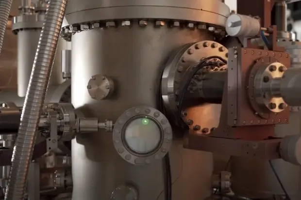
To achieve this level of atomic precision, MBE growth is performed in an ultra-high vacuum environment (UHV), where pressures as low as 10-¹² mbar (10−10 Pa) eliminate contamination. This purity level is achieved by using an array of pumps, such as turbo molecular pumps and ion getter pumps, which create conditions even cleaner than space.

Unmatched Infrastructure in Europe
With thirteen MBE reactors, PDI operates one of Europe’s largest collections of MBE systems. Each reactor is carefully assigned to a single material system to prevent cross-contamination, providing unmatched material quality. Most systems are housed within a 500 m² clean room designed for optimal conditions and contamination control.
- Cluster Systems: Several MBE reactors are integrated into cluster systems, enabling multi-material growth processes without exposure to air.
- Real-Time Analysis: One reactor is connected to the PHARAO facility at the synchrotron BESSY II (HZB), where in-situ, real-time x-ray diffraction enables PDI researchers to study growth dynamics at an atomic level.

Expanding MBE Applications
The versatility of MBE at PDI supports exploration across several advanced materials and applications, including:
- Oxides (e.g., Ga₂O₃, GeO₂, SrTiO₃) for optoelectronics and sensors
- Nanowires and Nanopillars (e.g., GaN, GaAs, AlN) for nano-electronic devices
- Quantum Cascade Lasers to drive next-generation photonic applications
- Magnetic Materials (e.g., FeGe, NiO, FGT) crucial for data storage and spintronic devices
Through these activities, PDI’s MBE expertise enables groundbreaking developments that inspire and demonstrate new functionalities for future technologies.
Presented by

Moritz Hansemann, MBE growth and Electron Microscopy