Metamaterials of the Future
With rising energy demands, even the most efficient devices waste a lot of energy due to material limitations. What if we could engineer a new class of materials to tackle this problem and drastically reduce energy waste? Dr. Abbes Tahraoui and Dr. Hans Tornatzky explore the promise of meta materials to revolutionize energy use.
Building the Future with 2D Materials
PDI’s research into two-dimensional (2D) materials supports the development of next-generation devices while exploring the fundamental science behind these ultra-thin structures. By studying materials like graphene, we can create layered van der Waals (vdW) heterostructures that unlock entirely new properties — phenomena that don’t occur in single materials alone. This work not only advances sustainable technology but also deepens our understanding of these remarkable materials at the atomic level.
What are 2D Materials and Why Do They Matter?
Graphene and other 2D materials are incredibly thin layers, just one or a few atoms thick, that hold big promise for making future devices more efficient. By stacking these ultra-thin layers, we can create new ‘meta materials’ with unique properties that can’t be found in single layers alone. For example, when we combine graphene with other layers, we open up possibilities for creating more efficient devices that use less energy and work faster.
2D materials are ideal for exploring hetero-material systems, revealing insights into layer interactions and enabling the discovery of high-efficiency and novel applications. Unlike conventional 2D structures (e.g., quantum wells in blue lasers), 2D materials have no dangling bonds, eliminating the need for passivation and enhancing stability. They also avoid lattice mismatch issues, allowing seamless integration. These advantages make 2D materials versatile candidates for next-generation applications in optoelectronics, energy harvesting, and beyond.

What are Moiré Patterns?
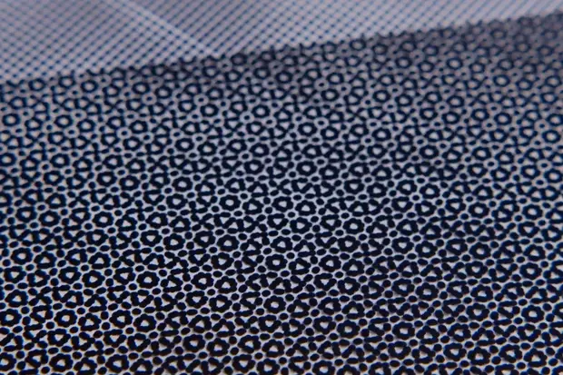
Moiré patterns are interference patterns that appear when two grids or layers with slight differences in alignment overlap. In 2D materials, Moiré patterns form when two atomically thin layers are stacked at a small angle or with mismatched lattice structures. These subtle misalignments can alter the electronic, optical, and magnetic properties of 2D materials, potentially leading to superconductivity or other novel electronic behaviors. This ability to ‘tune’ materials by adjusting the twist angle between layers makes Moiré patterns a powerful tool for developing next-generation devices.

How We Build and Test 2D Materials
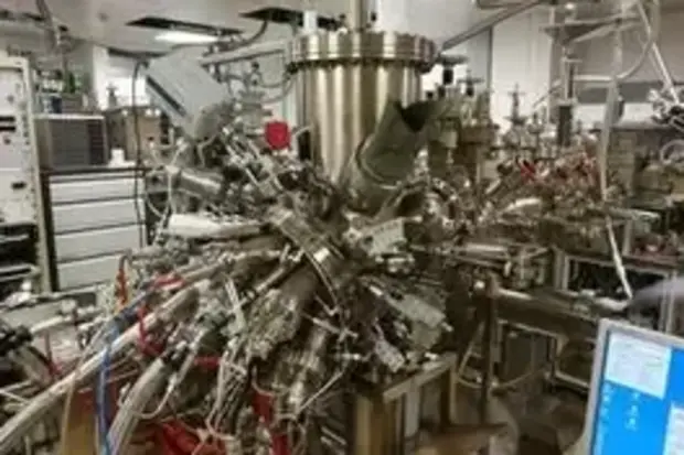
- Material Growth: We start by using Molecular Beam Epitaxy (MBE) to grow these layers with atomic-level precision.
- Characterization and Optimization: Advanced techniques like optical spectroscopy and electrical tests help us adjust growth parameters to optimize material properties.
- Device Design and Fabrication: With optimized materials, we design and build devices that align with our goals for energy efficiency and specific functionalities.
Innovations in 2D Materials for Energy-Efficient Devices
Our work takes two approaches: miniaturizing devices to outperform Moore’s Law and using new 2D materials to replace traditional silicon. While bringing experimental materials into real-world use remains challenging, combining smaller device structures with 2D materials allows us to unlock new functionalities. By engineering nanoscale features in these materials, we enhance their ability to harvest and convert energy, leading to more sustainable, high-performance electronics.
Why 2D Materials are Key to the Future of Technology
Epitaxial growth of 2D materials opens avenues for creating devices that consume less energy and rely on sustainable power sources. By combining graphene, hexagonal BN, and Te-based semiconductors, we explore how interlayer interactions, defect engineering, and lattice matching contribute to improved device performance. These materials hold promise not just for energy-efficient devices but for applications like quantum computing and sensing technologies, paving the way for the next generation of sustainable electronic devices.
Presented by

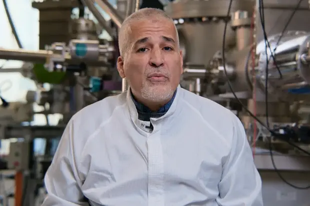
Dr. Abbes Tahraoui, MBE Growth & Device Technology

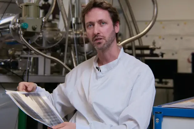
Dr. Hans Tornatzky, Optical Spectroscopy