2D materials
Graphene and other two-dimensional (2D) materials are promising building blocks for the fabrication of novel, atomically thin devices for future applications. In addition, combining them to form the so-called van der Waals (vdW) heterostructures enables novel, promising phenomena which are not observed in the single materials. For instance, in heterostacks composed of graphene and hexagonal BN (h-BN) layers the band structure of graphene can in principle be engineered via the design of stacking characteristics such as number of layers as well as crystallographic alignment.
For technological implementation, it is mandatory to synthesize these material systems with high precision, in particular sub-monolayer thickness control, in a scalable way—i.e. differently than by working with exfoliated, micrometer-sized flakes. Therefore, our activity mainly focuses on the epitaxial growth of graphene and h-BN, as well as of vdW heterostructures combining them. Recently, we also started integrating Te-based 2D materials exhibiting semiconducting and magnetic properties with graphene and h-BN into vdW heterostacks. Beyond the envisioned benefits for applications, epitaxial growth of 2D crystals is a rich research field in its own right, as nucleation and growth may not follow the traditional routes of epitaxy.
Molecular beam epitaxy (MBE) is employed by us to obtain controlled, large-area growth of these materials. In addition to graphene, we perform MBE of atomically thin h-BN films. The latter have been successfully employed as encapsulation layers for other 2D materials such as transition metal dichalcogenides, as well as large-area templates hosting luminescent defects acting as single photon emitters. Furthermore, MBE growth of vdW-bonded systems such as h-BN/graphene and Sb2Te3/graphene is also under investigation. Fundamental growth studies have already allowed us to identify unconventional phenomena such as defect-mediated nucleation and coincident-site lattice matching happening in vdW epitaxy. Such effects influence interlayer interactions, strain, and stacking order between the dissimilar 2D materials, which in turn directly affect the properties and functionalities of the material system.

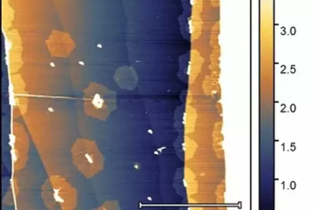
Beyond MBE, we also fabricate epitaxial graphene on SiC via surface graphitization. This type of sample is used as a 2D template to perform growth studies of different materials on graphene such as h-BN (as mentioned above), GaN nanowires, and thin films of the semiconducting oxides NiO and In2O3. The high crystalline quality, inertness, and atomic flatness of epitaxial graphene on SiC make it an ideal substrate for the development of growth protocols for vdW epitaxy.
Contact
Selected publications
Author: M. Heilmann , A. S. Prikhodko , M. Hanke , A. Sabelfeld , N. I. Borgardt , J. M. J. Lopes
Title: Influence of Proximity to Supporting Substrate on van der Waals Epitaxy of Atomically Thin Graphene/hexagonal Boron Nitride Heterostructures
Source: ACS Appl. Mater. Interfaces , 12 , 8897 ( 2020 )
DOI: 10.1021/acsami.9b21490
Author: S. Nakhaie , M. Heilmann , T. Krause , M. Hanke , J. M. J. Lopes
Title: Nucleation and growth of atomically thin hexagonal boron nitride on Ni/MgO(111) by molecular beam epitaxy
Source: J. Appl. Phys. , 125 , 115301 ( 2019 )
DOI: 10.1063/1.5081806
Author: E. Courtade , B. Han , S.Nakhaie , C. Robert , X. Marie , P. Renucci , T. Taniguchi , K. Watanabe , L. Geelhaar , J. M. J. Lopes , B. Urbaszek
Title: Spectrally narrow exciton luminescence from monolayer MoS2 and MoSe2 exfoliated onto epitaxially grown hexagonal BN
Source: Appl. Phys. Lett. , 113 , 032106 ( 2018 )
DOI: 10.1063/1.5033554
Author: A. Hernández-Mínguez , J. Lähnemann , S. Nakhaie , J. M. J. Lopes , P. V. Santos
Title: Luminescent Defects in a Few-Layer h-BN Film Grown by Molecular Beam Epitaxy
Source: Phys. Rev. Appl. , 10 , 044031 ( 2018 )
DOI: 10.1103/PhysRevApplied.10.044031
Author: M. Heilmann , M. Bashouti , H. Riechert , J. M. J. Lopes
Title: Defect mediated van der Waals epitaxy of hexagonal boron nitride on graphene
Source: 2D Mater. , 5 , 025004 ( 2018 )
DOI: 10.1088/2053-1583/aaa4cb