Controlling free electrons in quantum circuits
The progress of electronic devices is increasingly linked to the utilization of quantum effects. A future scenario are integrated quantum circuits containing coupled nanostructures. Interconnects, coupling distant on-chip components, could then be realized by the exchange of ballistic electrons. Our work aims at optimizing the coherent exchange of ballistic electrons between quantum point contacts, fundamental building blocks of quantum circuits.
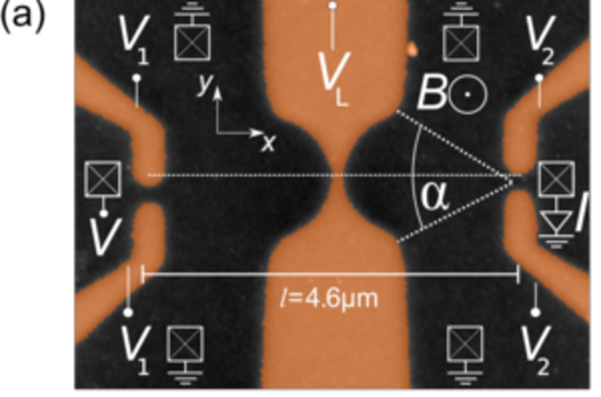
A quantum point contact is a narrow one-dimensional constriction in a two-dimensional conducting sheet. It is realized using the electric field effect by applying a voltage to control gates. The electrostatic potential forms a tunable barrier at the point contact, while the electrons are laterally confined giving rise to the famous quantization of the conductance in one dimension. A sample containing two point contacts (each defined by two gates) and a lens gate in between is shown in Fig. 1(a).
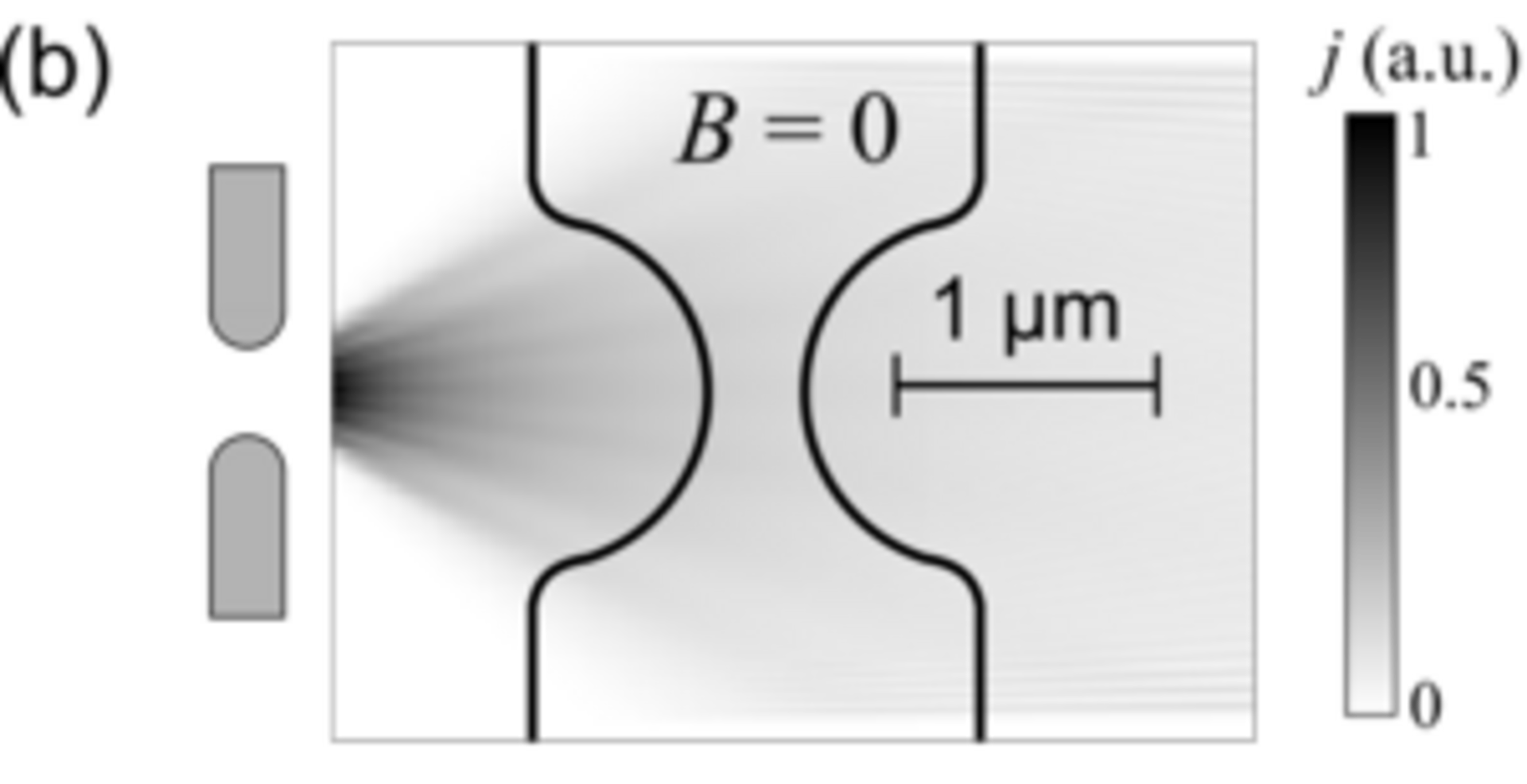
Electrons emitted from such a narrow aperture move within an expanding funnel, as a result of a numerical calculation in Fig. 1(b) demonstrates. The current density distribution thereby depends on the conductance of the point contact and its detailed geometry. Evidently, to enhance the exchange between two distant nanostructures, it would help to refocus the emitted electrons.
First, we studied the geometry of individual point contacts. It turns out that their effective local potential is increasingly influenced by the Coulomb interaction of free electrons inside the constriction as the conductance of the point contact is enhanced and it is populated by free electrons. The latter rearrange themselves and thereby partly screen the local electric field. Combining non-linear transport spectroscopy and numerical calculations, we show that this screening gives rise to a transition from an approximately parabolic lateral confinement of the almost pinched off point contact toward a square potential when the point contact is opened beyond a few quantized channels and populated by many free electrons [1].
Next, we measured the ballistic current through two point contacts in series [cf. Fig. 1(a)] as a function of the conductance of the point contacts and external parameters such as the magnetic field. We analyzed our results by comparison with the numerically calculated prediction of the Schrödinger equation for a free carrier. In particular, magnetic focusing experiments allowed us to explore the current emission profile of the point contacts. As the emission profile of a point contact depends characteristically on its geometry and conductance, these experiments can serve as an alternative path to determine and fine tune the electrostatic potential of a point contact [2].
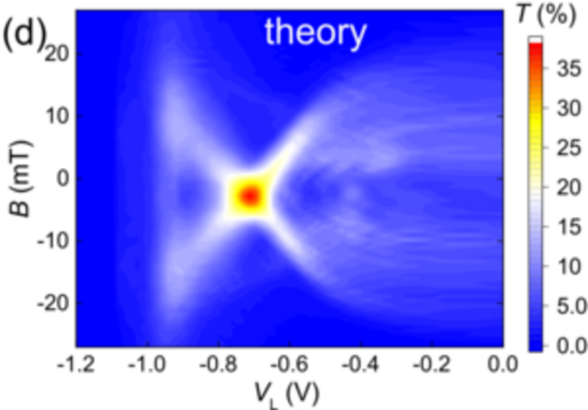
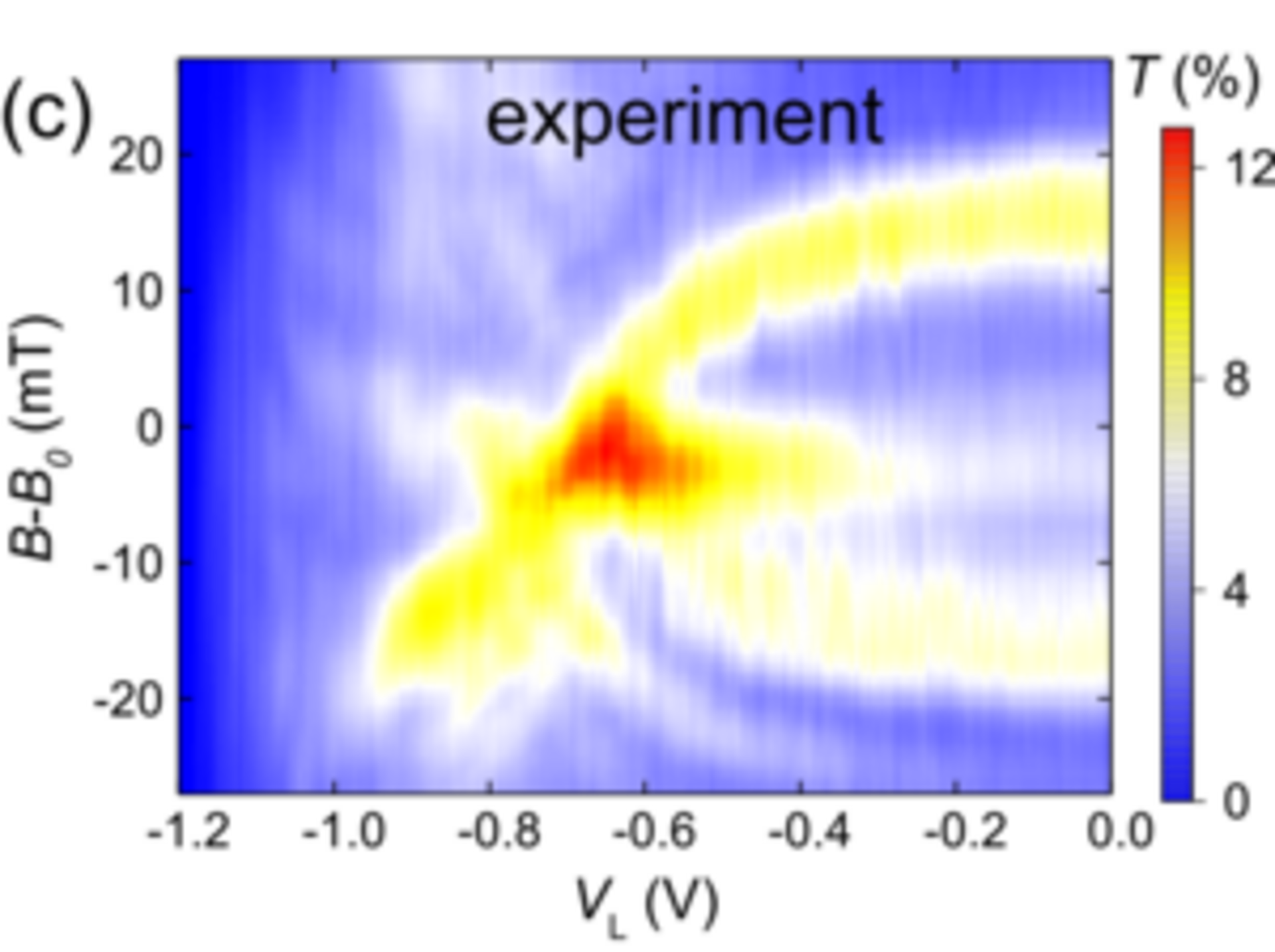
Finally, we added an electrostatic lens between the two point contacts with the purpose to enhance the coherent coupling between the two by refocusing of electrons emitted by one point contact. The electrostatic lens roughly resembles an optical lens, while instead of varying the speed of light we vary the Fermi velocity of the electrons by applying a voltage to the lens-shaped gate shown in Fig. 1(a). The focusing effect is visualized in Fig. 1(c), presenting the measured transmission through two point contacts in series as a function of the magnetic field B and the voltage VL applied to the lens gate. The transmission is thereby defined as the ratio of the currents flowing through both point contacts versus the emitter only. The experimental result qualitatively resembles the numerically calculated transmission shown in Fig. 1(d). At VL = 0, the current is distributed over a wide range of B values corresponding to a wide aperture angle of the emitted electrons. As VL is decreased, the current maxima move to lower magnetic fields and cumulate at VL ≅ 0.64 in a single enhanced maximum at B = 0. These data prove focusing, which corresponds to an enhanced electron exchange between the two distant nanostructures [2].
[1] Author: M. Geier, J. Freudenfeld, J. T. Silva, V. Umansky, D. Reuter, A. D. Wieck, P. W. Brouwer, and S. Ludwig
Title: Electrostatic potential shape of gate-defined quantum point contacts
Souce: Phys. Rev. B 101, 165429 (2020)
DOI: 10.1103/PhysRevB.101.165429
[2] Author: J. Freudenfeld, M. Geier, V. Umansky, P. W. Brouwer, and S. Ludwig
Title: Coherent electron optics with ballistically coupled quantum point contacts
Source: Phys. Rev. Lett. 125, 107701 (2020)
DOI: 10.1103/PhysRevLett.125.107701