Artificial quantum states on semiconductor surfaces created and probed by cryogenic scanning tunneling microscopy
01/02/2024 - 31/01/2027
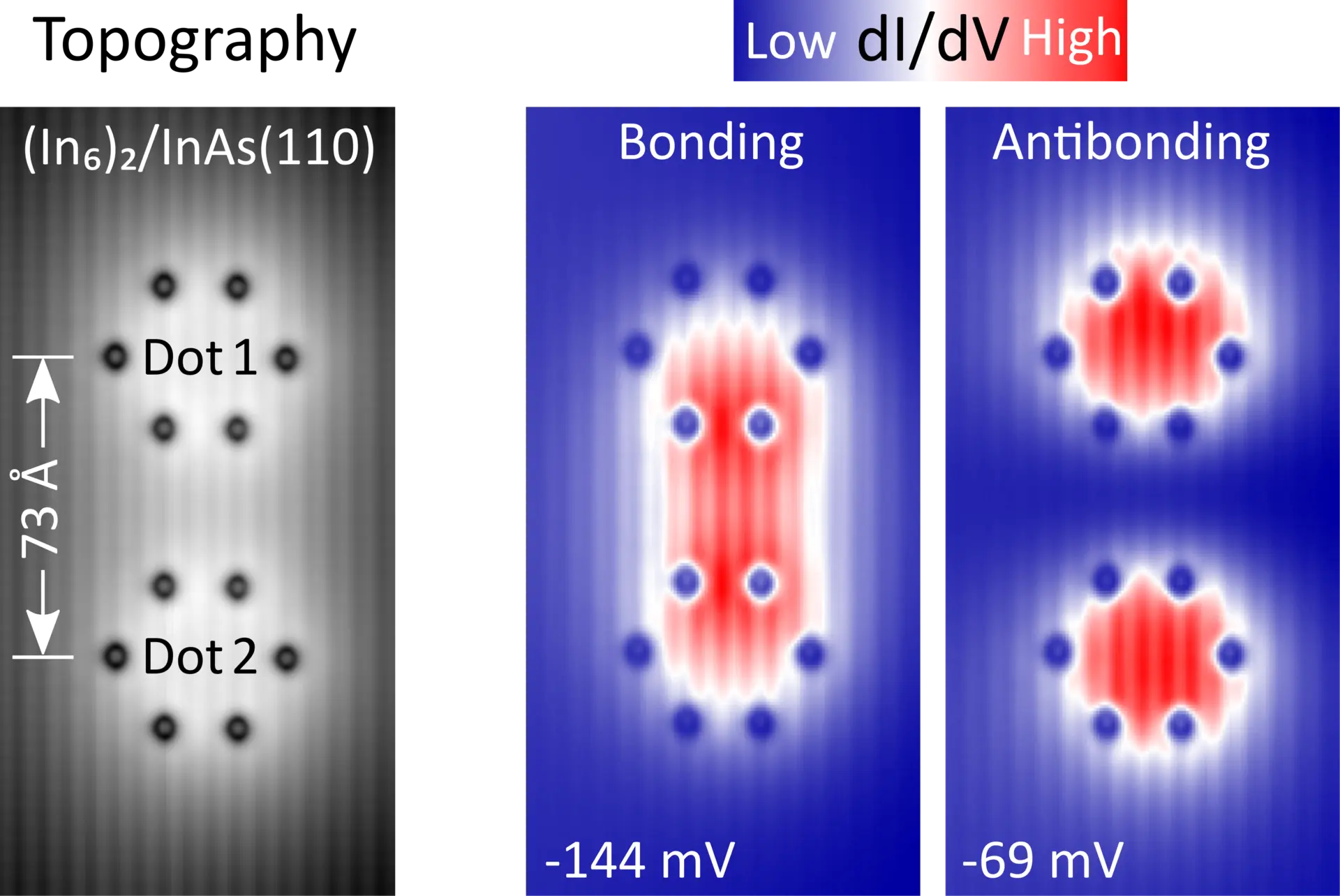
This project employs cryogenic scanning tunneling microscopy (STM) to create atom-based quantum structures on semiconductor surfaces and explore their electronic properties by scanning tunneling spectroscopy. The structures are assembled from ionized adatoms via atom manipulation on the InAs(111)A surface, leading to electrostatic carrier confinement on the atomic length scale. This method enables one to construct quantum dots with a perfectly defined level structure, as well as dot assemblies whose quantum coupling has no intrinsic variation but can nonetheless be tuned over a wide range. Among other achievements, we have implemented dimerized quantum-dot chains hosting electronic boundary states as predicted by the Su-Schrieffer-Heeger model of one-dimensional topological phases.
Building on our previous work, the goal is to extend the approach to (110)-cleaved InAs surfaces with large-scale, atomically flat terraces, facilitating the construction of more elaborate quantum-dot arrays hosting exotic electronic states. Additionally, working in (110) surface orientation offers the prospect of exploring cleaved III-V semiconductor heterostructures in cross-sectional geometry, ultimately enabling the creation of electrical gating of the STM-generated nanostructures. Perfectly defined and tunable surface structures on semiconductors provide detailed insight into the behavior of electrons in reduced dimensions – which is crucial for fundamental science and future quantum technologies based on engineered nanoscale materials.
This project is funded by the Deutsche Forschungsgemeinschaft (DFG) under Grants No. 437494632.
Contact
Selected Publications
-
- Title
-
Quantum dots on the InAs(110) cleavage surface created by atom manipulation
- Author
- V. D. Pham, Y. Pan, S. C. Erwin, S. Fölsch
- Source
- Phys. Rev. Research, 6, 013269 (2024)
- DOI:
- 10.1103/PhysRevResearch.6.013269 (PDI-ID: 2977)
-
- Title
-
Topological states in dimerized quantum-dot chains created by atom manipulation
- Author
- V. D. Pham, Y. Pan, S. C. Erwin, F. von Oppen, K. Kanisawa, S. Fölsch
- Source
- Phys. Rev. B, 105, 125418 (2022)
- DOI:
- 10.1103/PhysRevB.105.125418 (PDI-ID: 2809)