A New Orientation for Scandium Nitride
/ Announcements
Researchers at the Paul Drude Institute for Solid State Electronics (PDI) have opened up a completely new way of growing scandium nitride (ScN), a material with promising applications in electronics, thermoelectronics and optoelectronics. Until now, ScN has only been realized in the more conventional (001), (110), or (111) orientations. However, in a paper recently published in ACS Applied Electronic Materials, Duc V. Dinh, Esperanza Luna, and Oliver Brandt report the first successful growth of ScN thin films in the unusual (113) crystal orientation. This breakthrough not only expands the possibilities for nitride materials research but also creates fresh opportunities to fine-tune properties such as strain, interfaces, and anisotropy—factors that are essential for future device technologies.
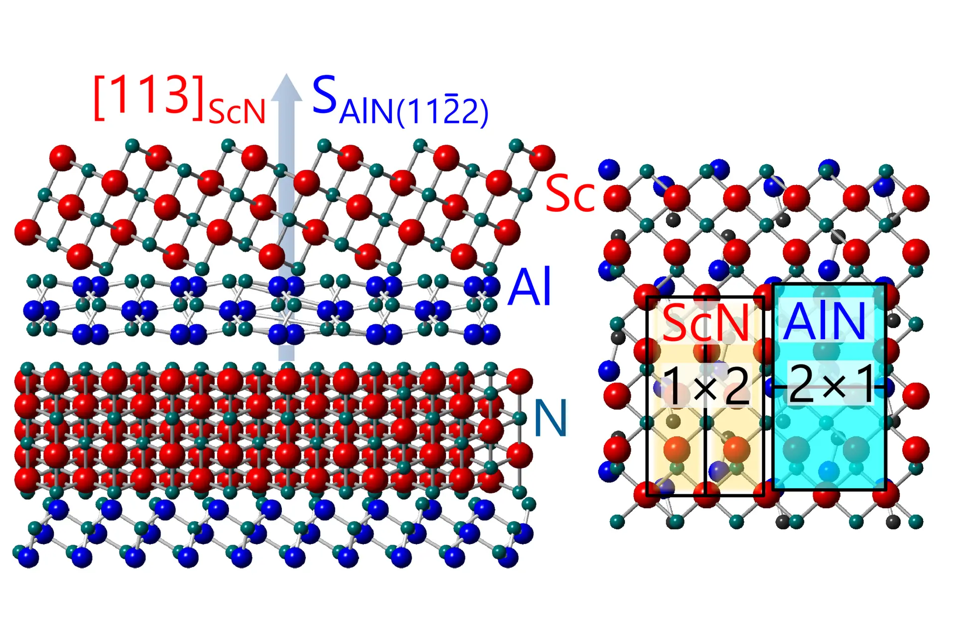
To achieve this result, the researchers used plasma-assisted molecular beam epitaxy to grow ScN layers on semipolar AlN(11̅22) templates prepared on Al2O3 substrates. They deposited undoped ScN layers with thicknesses ranging from 85 nm to 210 nm and examined their properties in detail. Structural characterization with X-ray diffraction and transmission electron microscopy (TEM) confirmed that the films have a single (113) orientation, although they exhibit rotational twin domains. Two distinct in-plane epitaxial relationships between ScN and the AlN template were identified, reflecting different strain conditions at the interface. High-resolution TEM imaging further revealed columnar grains coalesced during growth and that stacking faults in the AlN templates terminated at the ScN/AlN hetero-interface.
The researchers also investigated the optical and electronic behavior of the films. Photoluminescence measurements revealed a broad emission around 2.16 eV, consistent with transitions near the lowest direct gap at the X-point in the electronic band structure of ScN. Hall-effect measurements across a wide temperature range (4−380 K) showed that charge transport is dominated by conduction through the impurity bands. Analysis of the temperature dependence of mobility indicated that electron scattering is primarily governed by optical phonons, with an effective phonon energy of about 60 meV.
With this study, the team of researchers has demonstrated that it is possible to grow high-quality ScN in a crystal orientation that had never been achieved before. By carefully analyzing its structural, optical, and electrical properties, they have established a solid foundation for exploring how such “non-standard” orientations can influence material behavior. The results highlight not just a technical milestone in epitaxial growth, but also a new pathway for designing nitride-based materials with tailored properties. This opens exciting opportunities for future research and could ultimately help enable new generations of electronic and optoelectronic devices.
Title: Rock-Salt ScN(113) Layers Grown on AlN(112̅2) by Plasma-Assisted Molecular Beam Epitaxy
Authors: D. V. Dinh, E. Luna, O. Brandt
Source: ACS Appl. Electron. Mater. 2025, 7, 17, 8145–8154
DOI: 10.1021/acsaelm.5c01202
Core Research Area (CReA): Nitride Semiconductors