Nitride Semiconductors
The compound semiconductors indium, gallium and aluminum nitride and their alloys are the second most economically important class of semiconductors after silicon. For example, they form the basis of light-emitting diodes (LEDs) that have revolutionized the general lighting market in the past decade and for amplifiers and electronic switches in power electronics. The high efficiency of these components is an important factor for reducing the consumption of electrical energy.
PDI has a longstanding tradition in both producing high-quality epilayers of nitride semiconductors by molecular beam epitaxy and their detailed characterization, in particular using luminescence spectroscopy. Currently, we are pursuing three complementary research directions in this context, with a particular focus on materials with an ultra-wide band gap. Firstly, we are working on innovative electronic components based on high electron mobility transistors (HEMTs) utilizing aluminum nitride. Secondly, we explore the growth of novel nitride compounds. Alloys with transition metals such as scandium or chromium can enable new functionalities such as ferroelectricity and ferromagnetism. Boron nitride is highly relevant in heterostructures with two-dimensional materials, but also as potential host for room-temperature quantum emitters. Thirdly, we are investigating charge carrier recombination with the aim to understand basic material properties and to identify ways to improve optoelectronic components. In this context, the new application laboratory for time-resolved cathodoluminescence spectroscopy (ZALKAL) plays a central role as it is specially designed for semiconductors with an ultra-wide band gap.
Scientific Highlights
A New Orientation for Scandium Nitride
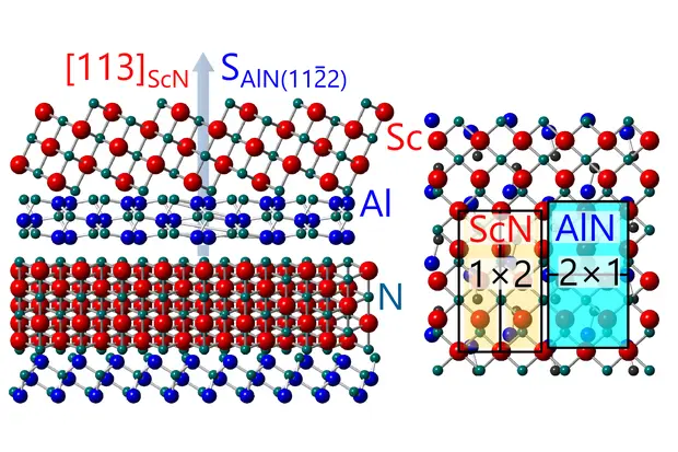
PDI researchers have achieved the first epitaxial growth of scandium nitride in the unusual (113) orientation, expanding the possibilities for nitride materials research. Published in ACS Applied Electronic Materials, this breakthrough opens new pathways for designing nitride-based materials with tailored properties for future electronic and optoelectronic applications. More…
PDI Researchers Achieve Thick (In,Ga)N Layers with Uniform Composition and Low Dislocation Density Using MBE
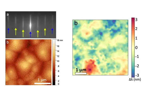
A new study by researchers at the Paul-Drude-Institut für Festkörperelektronik (PDI), published in Journal of Physics D: Applied Physics, demonstrates a major advancement in the growth of high-quality indium gallium nitride (InₓGa₁₋ₓN) layers using plasma-assisted molecular beam epitaxy (MBE). More…
Electrical properties of ScN(111) layers grown on semi-insulating GaN(0001) by plasma-assisted molecular beam epitaxy
Researchers at the Paul Drude Institute for Solid State Electronics (PDI) have investigated the electrical properties of nominally undoped scandium nitride (ScN) layers grown on semi-insulating gallium nitride (GaN) substrates using plasma-assisted molecular beam epitaxy (MBE). The study, published in Physical Review Applied, focuses on 10–40 nm thick ScN(111) layers deposited on nearly lattice-matched GaN(0001) templates. Full article available via APS (subscription required)
Generation of GHz Surface Acoustic Waves in (Sc,Al)N Thin Films on Polycrystalline Diamond
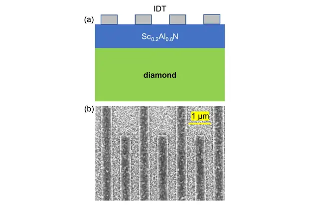
Researchers from PDI, in collaboration with partners from Cardiff University and other institutions, have demonstrated the generation of surface acoustic waves (SAWs) with frequencies up to 8 GHz in scandium aluminum nitride (Sc₀.₂Al₀.₈N) thin films grown on free-standing polycrystalline diamond wafers. The study, published in Journal of Physics D: Applied Physics, utilized plasma-assisted molecular beam epitaxy (MBE) to deposit the (Sc,Al)N films, aiming to establish a platform for high-frequency SAW devices. Read article…
Third-party Funded Projects
- Application laboratory time-resolved cathodoluminescence spectroscopy (ZALKAL)
- Defect-engineering in graphene via focused ion beam for tailored van der Waals epitaxy of h-BN (ENGRAVE)
- Complementary Electron Microscopy Techniques for Efficient AlGaN Optoelectronics (DAAD Procope, with Institut Néel)
Selected Publications
2025
- Growth of compositionally uniform InxGa1−xN layers with low relaxation degree on GaN by molecular beam epitaxy
Authors: J. Kang, M. Gómez Ruiz, D. V. Dinh, A. Campbell, P. John, T. Auzelle, A. Trampert, J. Lähnemann, O. Brandt, L. Geelhaar
Source: J. Phys. D: Appl. Phys., 58, 14LT01 (2025)
DOI: 10.1088/1361-6463/adb4e7
2024
- Electrical properties of ScN(111) layers grown on semi-insulating GaN(0001) by plasma-assisted molecular beam epitaxy
Authors: D. V. Dinh, O. Brandt
Source: Phys. Rev. Appl., 22, 014067 (2024)
DOI: 10.1103/PhysRevApplied.22.014067
- Generation of GHz surface acoustic waves in (Sc,Al)N thin films grown on free-standing polycrystalline diamond wafers by plasma-assisted molecular beam epitaxy
Authors: M. Yuan, D. V. Dinh, S. Mandal, O. A. Williams, Z. Chen, O. Brandt, P. V. Santos
Source: J. Phys. D: Appl. Phys., 57, 495103 (2024)
DOI: 10.1088/1361-6463/ad76ba
- Multimode emission in GaN microdisk lasers
Authors: M. L. Drechsler, L. Sung-Min Choi, F. Tabataba-Vakili, F. Nippert, A. Koulas-Simos, M. Lorke, S. Reitzenstein, B. Alloing, P. Boucaud, M. R. Wagner, F. Jahnke
Source: Laser Photonics Rev., 18, 2400221 (2024)
DOI: 10.1002/lpor.202400221
2023
- Excitonic and deep-level emission from N- and Al-polar homoepitaxial AlN grown by molecular beam epitaxy
Authors: L. van Deurzen, J. Singhal, J. Encomendero, N. Pieczulewski, C. S. Chang, Y. Cho, D. A. Muller, H. G. Xing, D. Jena, O. Brandt, J. Lähnemann
Source: APL Mater., 11, 081109 (2023)
DOI:10.1063/5.0158390
- Lattice parameters of ScxAl1−xN layers grown on GaN(0001) by plasma-assisted molecular beam epitaxy
Authors: D. V. Dinh, J. Lähnemann, L. Geelhaar, O. Brandt
Source: Appl. Phys. Lett., 112, 152103-1 (2023)
DOI: 10.1063/5.0137873


