PDI Researchers Achieve Thick (In,Ga)N Layers with Uniform Composition and Low Dislocation Density Using MBE
/ Announcements
A new study by researchers at the Paul-Drude-Institut für Festkörperelektronik (PDI), published in Journal of Physics D: Applied Physics, demonstrates a major advancement in the growth of high-quality indium gallium nitride (InₓGa₁₋ₓN) layers using plasma-assisted molecular beam epitaxy (MBE).
Key Results
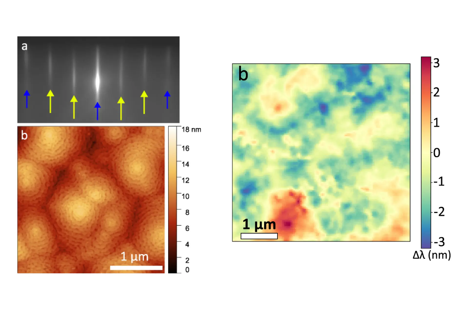
- Excellent Compositional Uniformity: The team successfully grew InₓGa₁₋ₓN layers with indium content ranging from x = 0.06 to 0.14. The In content of 500 nm-thick layers were highly uniform both laterally and along the growth direction.
- Low Degree of Relaxation: Even with indium content x > 0.1, the 500 nm-thick layers remained mostly strained—important for preserving crystal quality.
- Low Dislocation Densities: Cathodoluminescence and TEM measurements revealed low densities of threading dislocations (~1 × 10⁹ cm⁻²), a key metric for high quantum efficiency.
These results mark a critical step toward enabling top-down fabrication of bulk InₓGa₁₋ₓN nanowires ensembles with highly uniform properties and high quantum efficiency. The work opens new opportunities for the use of bulk InₓGa₁₋ₓN nanowires in photoelectrochemical applications, LEDs, and other optoelectronic devices.
Title: Growth of compositionally uniform InxGa1−xN layers with low relaxation degree on GaN by molecular beam epitaxy
Authors: J. Kang, M. Gómez Ruiz, D. V. Dinh, A. Campbell, P. John, T. Auzelle, A. Trampert, J. Lähnemann, O. Brandt, L. Geelhaar
Source: J. Phys. D: Appl. Phys., 58, 14LT01 (2025)
DOI: 10.1088/1361-6463/adb4e7
Core Research Area (CReA): Nitride Semiconductors and III-V Nanowires for Optoelectronics