III-V Nanowires for Optoelectronics
Semiconductor nanowires are ultra-thin structures with diameters typically smaller than 100 nm and an extremely high aspect ratio. These quasi-one-dimensional materials exhibit unique properties resulting from their nanoscale size, such as enhanced light-matter interaction and carrier confinement. Nanowires can be fabricated using bottom-up approaches like molecular beam epitaxy (MBE), achieving feature sizes down to 10 nm without lithography. Top-down methods offer greater precision, particularly in creating regular nanowire arrays. Regardless of the fabrication approach, nanowires display distinct advantages, including the ability to integrate multiple materials within a single structure, making them ideal for various optoelectronic applications.
The goal of our research is to explore and harness the functionalities of III-V nanowires for advanced optoelectronic devices. We focus on fundamental properties, such as microstructure, optical characteristics, and electronic behavior, that directly influence performance in applications like LEDs, lasers, and photodetectors. By growing both group-III-nitride and group-III-arsenide nanowires, we aim to gain insights into how their material composition and structural properties impact device efficiency.
Through this work, we seek to push the boundaries of optoelectronics by developing nanowire-based devices with improved performance, such as higher efficiency, lower power consumption, and better integration with existing technologies. Our research will contribute to advancing novel approaches in energy-efficient devices, high-speed optical communication, and next-generation quantum photonics.
Scientific Highlights
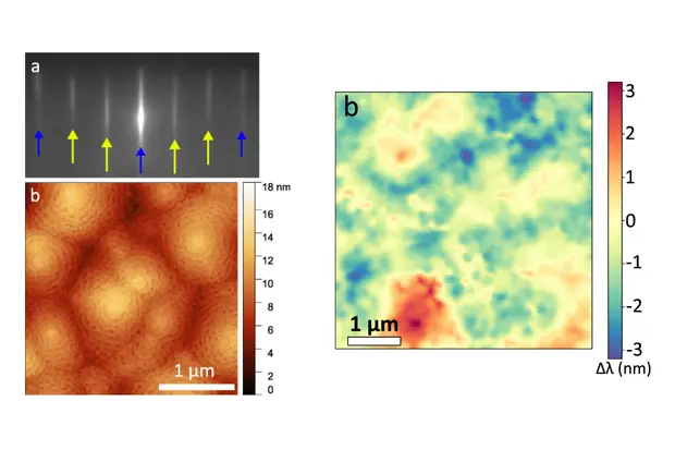
PDI Researchers Achieve Thick (In,Ga)N Layers with Uniform Composition and Low Dislocation Density Using MBE
A new study by researchers at the Paul-Drude-Institut für Festkörperelektronik (PDI), published in Journal of Physics D: Applied Physics, demonstrates a major advancement in the growth of high-quality indium gallium nitride (InₓGa₁₋ₓN) layers using plasma-assisted molecular beam epitaxy (MBE). More…
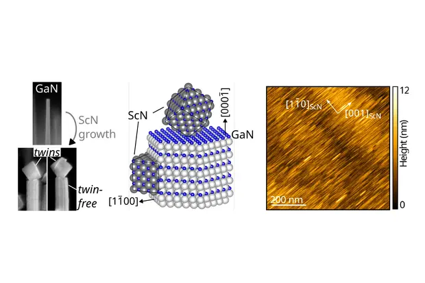
Epitaxy of highly dissimilar transition metal nitride-semiconductor heterostructures with low defect density
This study demonstrates twin-free epitaxial growth of rocksalt ScN on wurtzite GaN. Our approach opens a new route to combine wurtzite III-nitrides (AlN, GaN, InN) with rocksalt transition metal nitrides (ScN, ZrN, HfN, TiN, CrN, NbN) with unprecedented structural quality. This successful integration of transition metal nitrides on group III-nitrides with low defect densities offers new opportunities to enhance existing devices or develop innovative ones. More…
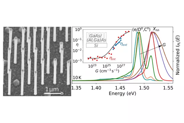
Carrier Recombination in Highly Uniform and Phase-Pure GaAs/(Al,Ga)As Core/Shell Nanowire Arrays on Si(111)
This work reports the growth of highly uniform, phase-pure GaAs/(Al,Ga)As nanowire arrays on silicon using molecular beam epitaxy. Their optical analysis reveals a sharp Mott transition and high quantum efficiency, highlighting the potential of these nanowires for efficient light-emitting devices integrated directly on silicon. More…
The azimuthal cell arrangement in molecular beam epitaxy drastically affects the luminescence efficiency of nanowire shells
The chamber geometry of a system for molecular beam epitaxy (MBE) is known to affect technical aspects such as the macroscopic deposition homogeneity across a wafer. However, for the microscopic mechanisms governing the growth of thin films on a planar substrate, the chamber geometry does not play any role. In marked contrast, we show here that the luminescence efficiency of (In,Ga)As/GaAs shell quantum wells grown around GaAs nanowires changes by more than two orders of magnitude depending on the relative position of the As cell compared to the group-III cells. More…
Understanding exciton recombination in GaN nanowires
A strong asset of bottom-up nanowires and related nanowire heterostructures is the enhanced surface strain relaxation that delays the onset of plastic relaxation. GaN nanowires that are free of dislocations can be directly grown on technologically relevant substrates such as silicon or metals. Yet, in spite of their high structural perfection, the electron-hole recombination in these nanoscopic structures remains predominantly nonradiative, even at cryogenic temperature. Here, we provide first evidence that the efficient nonradiative channel does not take place at point defects located at the nanowire surface or in the bulk, but stems instead from field-ionization of the exciton in the surface electric field. More…
GaAs-based nanowire heterostructure for light generation in the telecommunication O band on Si
The monolithic integration of light emitters on Si remains an important technological challenge for the development of intra-chip optical connections, as well as inter-chip connections. In this context, GaAs nanowires grown on Si substrates offer great potential, but their effective use for Si photonics technologies requires operation in the Si transparent window, with special relevance of the telecommunication bands for potential data transfer applications. Here, we present a novel coaxial nanowire heterostructure to extend the emission range of GaAs-based nanowire devices into the telecommunication O band. More…
Third-party Funded Projects
- Charge carrier dynamics under the influence of extreme strain gradients realized in bent semiconductor nanowires (DFG, with Universität Siegen)
- Photoelectrochemical CO2 reduction based on ordered (In,Ga)N NW arrays (DFG, with Helmholtz-Zentrum Berlin)
- Application laboratory time-resolved cathodoluminescence spectroscopy (ZALKAL)
- Lead-free piezoelectric nanowire-nanocellulose hybrids for flexible energy harvesters (Nanoflex)
- Large-area top-down processing of (In,Ga)N and (Al,Ga)N nanowires (DAAD, with Institut Néel)
Selected Publications
2024
- ScN/GaN(1-100): a new platform for the epitaxy of twin-free metal-semiconductor heterostructures
Authors: P. John, A. Trampert, D. V. Dinh, D. Spallek, J. Lähnemann, V. Kaganer, L. Geelhaar, O. Brandt, T. Auzelle
Published in: Nano Lett., 24, 6233 (2024)
DOI: https://doi.org/10.1021/acs.nanolett.4c00659
- AlN Nanowire-Based Vertically Integrated Piezoelectric Nanogenerators
Authors: N. Buatip, T. Auzelle, P. John, S. Rauwerdink, M. Sodhi, M. Salaün, B. Fernandez, E. Monroy, D. Mornex, C. R. Bowen, R. Songmuang
Published in: ACS Appl. Nano Mater., 7, 15798 (2024)
DOI: https://doi.org/10.1021/acsanm.4c03075
- Detection of an unintentional Si doping gradient in site-controlled GaN nanowires grown using a Si3N4 mask by spatially-resolved cathodoluminescence and Raman spectroscopy
Authors: Mikel Gómez Ruiz, Matt Brubaker, Kris Bertness, Alexana Roshko, Hans Tornatzky, Manfred Ramsteiner, Oliver Brandt, Jonas Lähnemann
Published in: APL Mater. 12, 101123 (2024)
DOI: https://doi.org/10.1063/5.0233859
2023
- Carrier recombination in highly uniform and phase-pure GaAs/(Al,Ga)As core/shell nanowire arrays on Si(111): Mott transition and internal quantum efficiency
Authors: M. Oliva, T. Flissikowski, M. Góra, J. Lähnemann, J. Herranz, R. B. Lewis, O. Marquardt, M. Ramsteiner, L. Geelhaar, O. Brandt
Published in: ACS Appl. Nano Mater., 6, 15278–15293 (2023)
DOI: 10.1021/acsanm.3c03242
- Growth kinetics and substrate stability during high-temperature molecular beam epitaxy of AlN nanowires
Authors: P. John, M. Gómez Ruiz, L. van Deurzen, J. Lähnemann, A. Trampert, L. Geelhaar, O. Brandt, T. Auzelle
Published in: Nanotechnology, 34, 465605 (2023)
DOI: 10.1088/1361-6528/acefd8
- Density control of GaN nanowires at the wafer scale using self-assembled Si patches on sputtered TiN(111)
Authors: T. Auzelle, M. Oliva, P. John, M. Ramsteiner, L. Geelhaar, O. Brandt
Published in: Nanotechnology, 34, 375602 (2023)
DOI: 10.1088/1361-6528/acdde8
- A route for the top-down fabrication of ordered ultrathin GaN nanowires
Authors: M. Oliva, V. M. Kaganer, M. Pudelski, S. Meister, A. Tahraoui, L. Geelhaar, O. Brandt, T. Auzelle
Published in: Nanotechnology, 34, 205301 (2023)
DOI: 10.1088/1361-6528/acb949
- Sequential directional deposition of one-sided (In,Ga)N shells on GaN nanowires by molecular beam epitaxy
Authors: D. van Treeck, J. Lähnemann, G. Gao, S. Fernández Garrido, O. Brandt, L. Geelhaar
Published in: APL Mater., 11, 091120 (2023)
DOI: 10.1063/5.0168786


