High-Mobility 2DEG at Oxide Interface Enabled by Precise Interface Engineering
/ Announcements
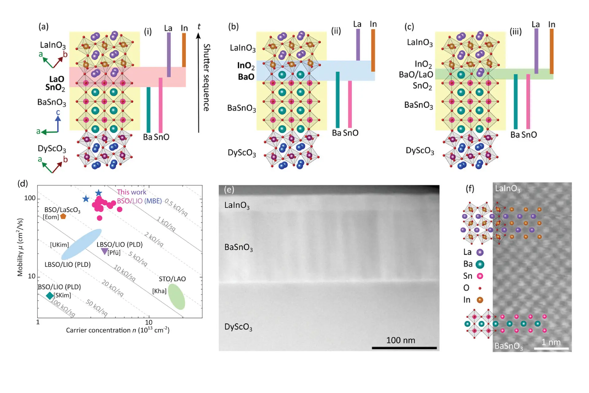
Researchers at the Paul Drude Institute for Solid State Electronics, in collaboration with the Leibniz-Institut für Kristallzüchtung (IKZ); University College London; University of Oxford; and the Deutsches Elektronen-Synchrotron DESY, report the formation of a two-dimensional electron gas (2DEG) with room-temperature electron mobility values up to 119 cm²/Vs at the interface between epitaxial layers of BaSnO₃ (BSO) and LaInO₃ (LIO). This mobility represents the highest value reported to date for a 2DEG in perovskite oxide systems at room temperature. The work, published in Advanced Materials, introduces a molecular beam epitaxy (MBE) growth protocol that enables controlled interface termination, a critical factor in achieving high mobility.
By combining adsorption-controlled co-deposition for bulk layer growth with shutter-controlled, layer-by-layer deposition of interfacial monolayers, the researchers engineered interfaces with specific terminations. Samples with a SnO₂/LaO-terminated interface exhibited reproducible charge carrier accumulation and high electron mobilities, verified through capacitance–voltage profiling and hard X-ray photoelectron spectroscopy. In contrast, heterostructures with BaO/InO₂ termination or undefined terminations did not show comparable electronic properties.
Electrical transport measurements confirmed that the interface termination governs the presence and quality of the 2DEG. SnO₂/LaO-terminated structures consistently yielded low sheet resistance and stable carrier concentrations, with mobility values exceeding 100 cm²/Vs. The study also demonstrated that the accumulation layer can be fully depleted with applied voltage, a feature relevant to potential device integration.
These findings establish interface termination as a key design parameter in oxide heterostructures and demonstrate a reproducible route for achieving high electron mobility in perovskite-based 2DEGs. The approach can be transferred to other perovskite oxide systems and provides a framework for further exploration of buried interfaces in electronic device structures.
Title: Enabling 2D electron gas with high room-temperature electron mobility exceeding 100 cm2 Vs−1 at a perovskite oxide interface
Authors: G. Hoffmann, M. Zupancic, A. A. Riaz, Curran Kalha, C. Schlueter, Andrei Gloskovskii, A. Regoutz, M. Albrecht, J. Nordlander, O. Bierwagen
Source: Adv. Mater., 36, 2409076 (2024)
DOI: 10.1002/adma.202409076
Core Research Area (CReA): Novel Functional Oxide Materials