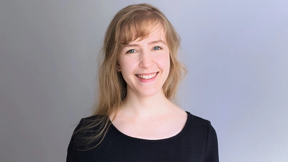
Introducing NanoNarratives — a series of conversations with the people at PDI. In the first of the series, we meet Ekaterina Paysen, a PhD student in the Microstructure department. Ekaterina won Best Student Oral Presentation at this year's International Conference on Silicon Epitaxy and Heterostructures and Silicon-Germanium Technology and Device Meeting (ISTDM-ICSI). She was recognized for her talk: 'Electron Tomography Analysis of Ge/SiGe Asymmetrically Coupled Quantum Wells'.
Can you share a little about your background?
I’m originally from Kyrgyzstan, but have lived and studied in Germany for most of my life. I studied in Berlin at the Technische Universität, starting out with a BSc in Natural Sciences in the Information Society, before I realized my passion for physics and began my bachelor's thesis in the field of electron microscopy.
What was it about PDI that attracted you?
When it was time to do my master’s thesis, I started looking for institutes outside of academia that offered electron microscopy, so that I could gain more experience in the field and learn how the work is carried out in other environments. I came across PDI when I started looking for Berlin-based institutes that offered this facility. I approached Dr. Achim Trampert (Head of Department of Microstructure) and asked if he had any interesting topics for me to investigate. I began investigating semiconductor heterostructures using quantitative scanning transmission electron microscopy and energy dispersive X-ray spectroscopy. Because PDI is so specialized, the groups tend to be small, which means you have more access to the instruments. I also enjoyed the relaxed working atmosphere and being able to learn from my colleagues. Looking back, this provided me with the time and the right circumstances to understand my results and learn more about electron microscopy in practice.
What is the topic of your PhD?
My PhD topic is related to electron tomography — a method used in electron microscopy. Using electron tomography, you retrieve a three-dimensional (3D) image of a sample, which also allows you to analyze its structural features in 3D. This is in contrast to conventional electron microscopy, where you only get two-dimensional projections of the sample and can run into interpretation difficulties because structural information is averaged over one of the three spatial dimensions. In my PhD research, I use this method to study the interfaces in semiconductor heterostructures or between semiconductors and superconductors grown by epitaxy.
Which groups are you collaborating with outside of PDI?
In the past, we have collaborated with Dr Sebastian Schütt's group at the Frauenhofer Institute for Applied Solid State Physics (IAF) on the three-dimensional characterization of (Ga,In)As/(Al,In)As interfaces in quantum cascade lasers (QCLs), and with Dr Rüdiger Schott from the Advanced Semiconductor Quantum Materials group at ETH Zürich on the characterization of InAs/Al interfaces in hybrid two-dimensional electron gas systems.[E.P.1]
Currently, we are collaborating with scientists from Italy. The collaboration originated through Giovanni Capellini — a professor at Dipartimento di Scienze, Università degli Studi Roma Tre, Rome, and a member of IHP – Leibniz-Institut für innovative Mikroelektronik, in Frankfurt (Oder). Professor Capellini contacted us because of a publication written by a former colleague at PDI, whose research I am progressing. The Italian colleagues are currently developing a Ge/GeSi THz Quantum Cascade Laser (QCL) and aim to obtain more 3D-resolved information about the Ge/GeSi interface properties for integration into the device engineering process. The Berlin Application Laboratory Electron Tomography (BALET) is one of only a handful of groups in the world using electron tomography on inorganic material systems. Our setup is specialized in electron tomography, which requires specific instruments and increased stability of the electron microscope. With our facilities, expertise, and our shared Leibnitz connection, it made sense that we would collaborate.
What is the focus of your current work?
At PDI, we don’t only carry out fundamental research, but also aim to demonstrate new functionalities through application; we work on devices that have a broad societal impact. In my work, I simultaneously focus on optimizing and understanding the method of electron tomography for investigation of semiconductor heterostructure interfaces. I am currently examining a Ge/Ge0.8Si0.2 multi-quantum well sample for our Italian colleagues, allowing me to generate new knowledge about the interface structure in this material system while demonstrating what electron tomography is capable of, thereby improving our understanding of the method. Unlike at university, at PDI I have the chance to work with groups who are closer to application. It’s a great opportunity. I still have a lot to learn and am grateful for the experience I’m gaining here.
What’s in the future for you and your career?
I would like to build a career outside of academia, in industry. I will move to Bavaria after my PhD and look for a suitable position there. I will be open to opportunities as they arise and would be pleased to continue my work in electron microscopy.
