PDI participates in new ANR–DFG funded project MINT
/ Announcements
We are pleased to announce that PDI scientist Dr. Philipp John, together with collaborators Dr. Ileana Florea (PI), Dr. Blandine Alloing, and Dr. Pierre-Marie Coulon from CNRS-CRHEA (Centre de Recherche sur l’Hétéro-Épitaxie et ses Applications), have been successfully awarded funding through the ANR–DFG program for their new collaborative project MINT. The collaboration underscores PDI’s ongoing commitment to innovation through strategic partnership and to addressing key scientific challenges that shape the future of advanced electronic and photonic technologies.
The ANR–DFG program is a joint initiative between the Agence Nationale de la Recherche (ANR) in France and the Deutsche Forschungsgemeinschaft (DFG) in Germany. It supports outstanding binational research collaborations across all scientific disciplines, fostering the integration of complementary expertise and infrastructure to strengthen the European Research Area (ERA).
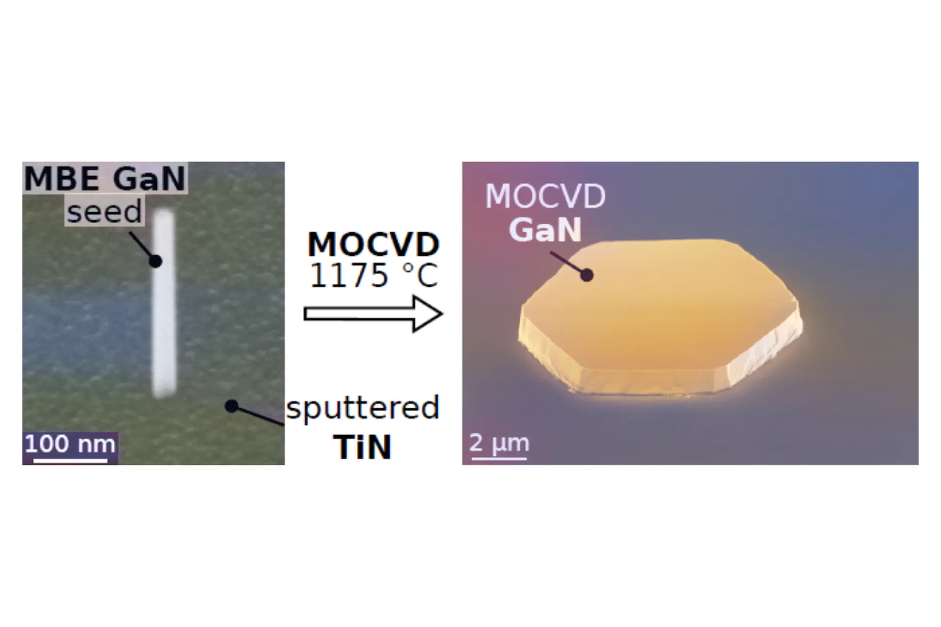
The project MINT – Monolithic Integration of Group-III Nitrides on Metallic TiN: A Path Towards Advanced (Opto-)Electronics aims to demonstrate novel types of group-III nitride-based (opto-)electronic devices by developing a fully epitaxial semiconductor-on-metal platform. Conductive TiN thin films serve as integrated bottom electrodes to power GaN-based micro light-emitting diodes (µLEDs) and AlN-based bulk acoustic wave devices. This innovative concept reduces device processing mainly to top contact deposition, resulting in an active region vertically powered between two electrodes. During device operation, the TiN bottom electrode additionally provides effective heat dissipation and back-reflection of emitted light.
To ensure high crystalline quality despite the chemical and structural differences between metal and semiconductor, the project employs molecular beam epitaxy (MBE) to grow defect-free GaN and AlN seed nanowires on refractory TiN films. Subsequent lateral overgrowth by metal-organic chemical vapor deposition (MOCVD) yields either hexagonally shaped µ-platelets or fully coalesced GaN and AlN layers. Structural and optical investigations will reveal the formation of possible defects at the semiconductor–metal interface and provide valuable feedback for optimizing growth conditions and nanowire morphology. In the final phase, the team will explore the integration of this approach on Si substrates, paving the way for scalable, industrially relevant applications.
This bilateral ANR–DFG funding instrument is part of Europe’s broader strategy to enhance research excellence, innovation, and global competitiveness. By joining forces through this German–French initiative, PDI contributes to strengthening the European Research Area (ERA) and advancing Europe’s technological leadership in semiconductor and materials science.