Nanoanalytics
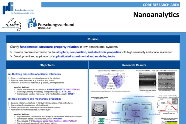
As opto-electronic technology continues to shrink device sizes, precise information on the structure and composition of low-dimensional systems and nanoscale devices becomes essential. The physical properties of the materials are often determined by atomic-scale features, making advanced characterization techniques crucial. This Core Research Area focuses on understanding the fundamental structure-property relation of nanomaterials through high-sensitivity, high-resolution experimental and modeling tools.
This CReA aims to:
- Clarify the structure-property relationship in low-dimensional systems.
- Provide precise information on the structure, composition, and electronic properties of nanoscale materials.
- Develop and apply sophisticated experimental and modeling tools for atomic-scale materials analysis.
Key research areas include:
- Epitaxial interfaces and 2D layers: Investigating hetero-interfaces in three dimensions (BALET), interfaces in van der Waals systems and intercalated layers, and extreme heteroepitaxy (PHARAO), exploring the electronic structure of cleaved heterostructures by scanning-probe techniques.
- Strain and defect characterization: Understanding strain relaxation mechanisms in anisotropic systems and displacement-induced deformation and (point) defects in 2D materials.
- Phase stability and phase transition in epitaxial systems: Studying composition fluctuations, disorder phenomena, and solid-phase epitaxy processes.
- Artificial quantum structures: Engineering quantum materials and manipulating atomic structures.
This research leverages PDI’s state-of-the-art signature labs and facilities, including Application Laboratory Electron Tomography (BALET), the PHARAO beamline (BESSYII, Helmholtz-Zentrum Berlin), and Low-Temperature Scanning Tunneling Microscopy (LT-STM), to push the limits of material characterization and manipulation.
Scientific Highlights
Silver Monolayer Defects, Vacancies and Impurities, Exhibit Dynamic Behavior under Electron Excitation
Featured in Quantum Zeitgeist: Van Dong Pham from the Paul-Drude-Institut für Festkörperelektronik, alongside Arpit Jain and Chengye Dong from Pennsylvania State University, and colleagues, demonstrate unprecedented control over atomic-scale defects within a single layer of silver positioned between graphene and silicon carbide. The work offers exciting possibilities for both fundamental research and technological applications. Read more…
Improving mobility in InAs quantum wells on GaAs substrate
Featured in Semiconductor Today: Researchers in Germany have reported improved mobility in indium arsenide (InAs) quantum wells (QWs) on gallium arsenide (GaAs) substrates, particularly at cryogenic temperatures less than 120K, from a surface smoothing technique used during molecular beam epitaxy (MBE). The team from Humboldt-Universität zu Berlin, Institut Kurz GmbH, and Paul-Drude-Institut für Festkörperelektronik, see their achievements as particularly interesting for quantum information processing.
Carrier diffusion length in GaN revisited
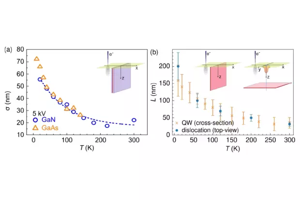
A figure of merit for the potential performance of any bipolar semiconductor device is the carrier diffusion length. For the technologically secondmost relevant semiconductor GaN, popular ways to determine this quantity using cathodoluminescence (CL) have been found to be based on incomplete physical models. This background motivates us to take a fresh, in-depth look on how to determine the carrier diffusion length in GaN using CL spectroscopy. More…
Strategies for Analyzing Non-Common-Atom Heterovalent Interfaces
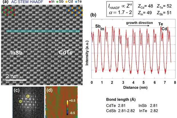
Semiconductor heterostructures are intrinsic to a wide range of modern-day electronic devices, such as computers, light-emitting devices and photodetectors. Knowledge of chemical interfacial profiles in these complex structures is critical to the task of optimizing the device performance. Here, we report on an innovative methodology that enables reliable interface structure analysis of non-common-atom heterovalent interfaces on all relevant length scales from hundred-nm to atomic resolution. More…
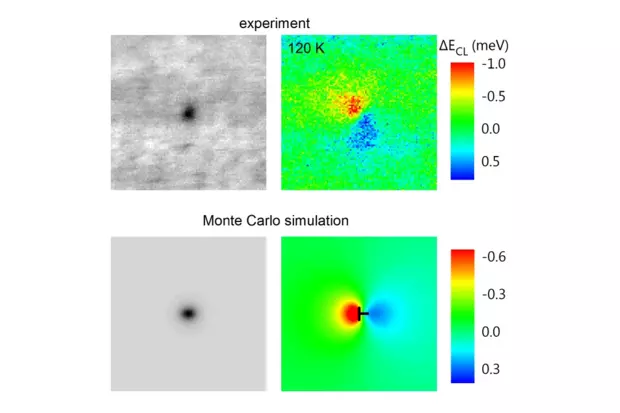
Can we determine the carrier diffusion length in GaN from cathodoluminescence maps around threading dislocations?
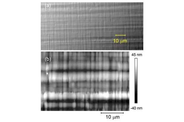
A popular method to experimentally determine the diffusion length of minority carriers or excitons in semiconductors relies on the perception that threading dislocations are line defects that act as nonradiative sinks for carriers. The zone of reduced luminescence intensity around the dislocation is thus directly related to the carrier or exciton diffusion length. Here, we show that this understanding of a diffusion-controlled intensity contrast around threading dislocations in GaN{0001} is a misconception. More…
Selected Publications
2025
- Strain relief and threading dislocation reduction in GaSb/AlSb/GaSb heterostructures grown on Si(001) substrate
Authors: K. Graser, A. Gilbert, J.-B. Rodriguez, E. Tournié, A. Trampert
Source: J. Appl. Phys., 137, 205302 (2025)
DOI: 10.1063/5.0268051
- Vibration-assisted tunneling through single Au adatoms on two-dimensional WSe2
Authors: H. Kumar, Y. C. Lin, J. A. Robinson, S. Fölsch
Source: Phys. Rev. B, 112, 085414 (2025)
DOI: 10.1103/nfd8-xrc4
2024
Scanning tunneling microscopy of ultrathin indium intercalated between graphene and SiC using confinement heteroepitaxy
Authors: V. D. Pham, C. González, Y. J. Dappe, C. Dong, J. A. Robinson, A. Trampert, R. Engel-Herbert
Source: Appl. Phys. Lett., 125, 181602 (2024)
DOI: 10.1063/5.0223972- Three-dimensional reconstruction of interface roughness and alloy disorder in Ge/GeSi asymmetric coupled quantum wells using electron tomography
Authors: E. Paysen, G. Capellini, E. Talamas Simola, L. Di Gaspare, M. De Seta, M. Virgilio, A. Trampert
Source: ACS Appl. Mater. Interfaces, 16, 4189-4198 (2024)
DOI: 10.1021/acsami.3c15546
- Detection of Bi_Ga hetero-antisites at Ga(As,Bi)/(Al,Ga)As interfaces
Authors: E. Luna, J. Puustinen, J. Hilska, M. Guina
Source: J. Appl. Phys., 135, 125303 (2024)
DOI: 10.1063/5.0195965
- Quantum dots on the InAs(110) cleavage surface created by atom manipulation
Authors: V. D. Pham, Y. Pan, S. C. Erwin, S. Fölsch
Source: Phys. Rev. Research, 6, 013269 (2024)
DOI: 10.1103/PhysRevResearch.6.013269
2023
