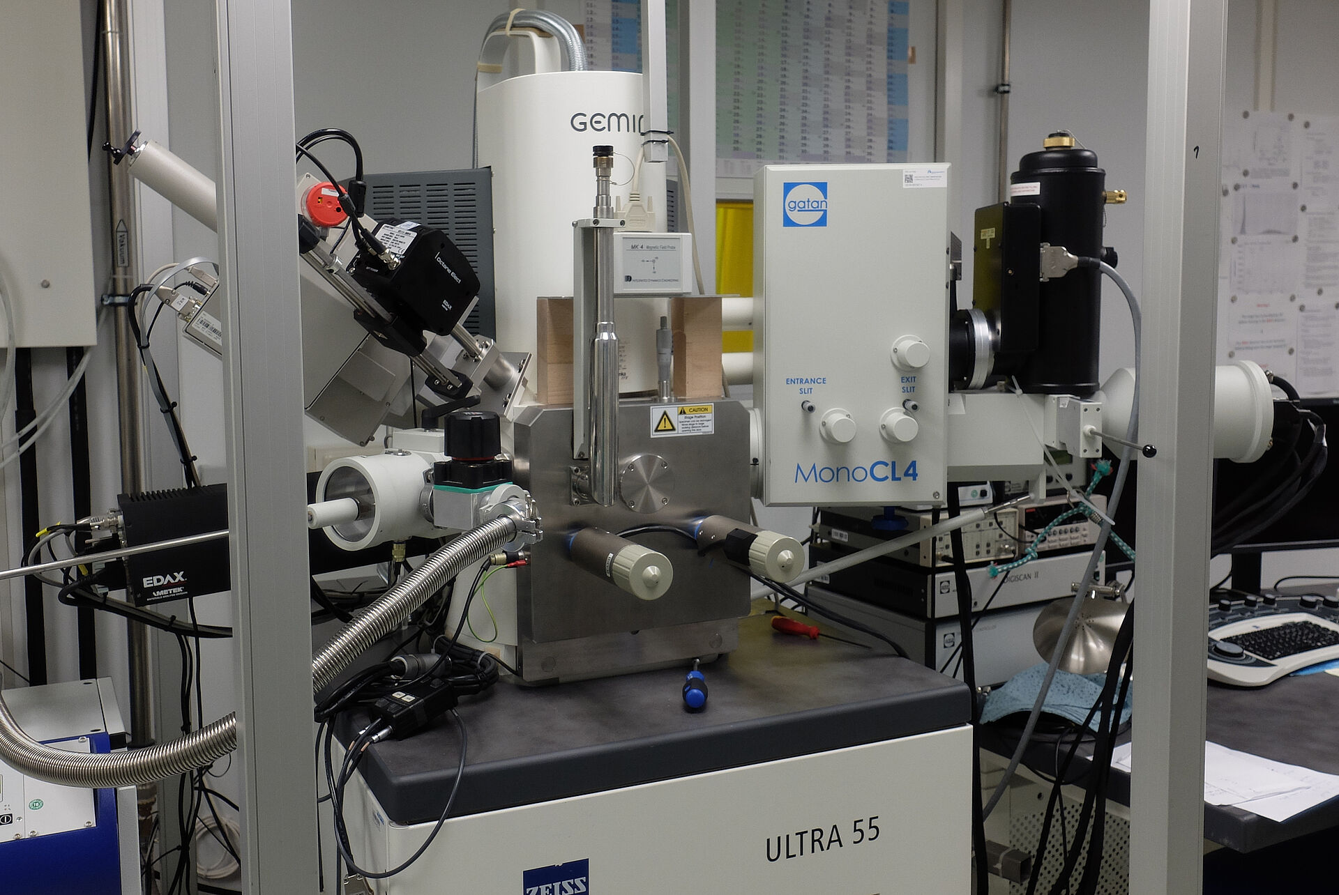
Cathodoluminescence Spectroscopy / Analytical Scanning Electron Microscope
Cathodoluminescence (CL) spectroscopy and imaging can be performed using a field-emission scanning electron microscope (FE-SEM) with a spatial resolution down to the nanometer range. In semiconductors, the incident electron beam in an SEM excites carriers from the valence to the conduction band. The subsequent relaxation of carriers results in light emission, which can then be analyzed by the spectrometer.
Thus, the system allows spatially resolved optical spectroscopy of semiconductor layers and micro- as well as nanostructures. The spectra convey information on heterostructures, defects, etc. Our system is especially optimized for the visible wavelength range, but also reaches into the UV and near-IR. A further advantage of CL spectroscopy in an SEM is the possibility to simultaneously acquire other signals, e.g. secondary electrons (SE) or electron beam induced current (EBIC) in addition to the CL spectrum or intensity, while the electron beam scans a certain region of the sample. Thus, different properties such as the surface morphology and electrical properties can be directly compared to the CL distribution. Furthermore, due to the high energy of the electron beam, CL is particularly well suited for the investigation of wide-gap materials. The variation of the electron beam acceleration voltage allows to choose the excitation depth and influences the spatial resolution which is determined both by electron scattering and carrier diffusion.
The analytical SEM is further equipped with an electron backscatter diffraction (EBSD) detector for the study of crystallographic orientation and strain and both an energy dispersive X-ray (EDX) detector as well as a wavelength dispersive X-ray (WDX) spectrometer used for element identification and compositional mapping.
SEM specifications:
- Acceleration voltages: 0.1-30 kV
- Beam currents: 10 pA - 20 nA
CL specifications:
- Wavelength range spectral mapping (CCD): 230-1080 nm
- Wavelength range monochromatic (PMT): 200-900 nm (up to 1700 nm with IR-PMT)
- Temperature range: 6-300 K
- Simultaneous EBIC acquisition
Complementary measurement techniques:
- EDX: 70 mm² silicon drift detector with Si₃N₄ window
- WDX: low-energy X-ray spectrometer for 0.08-2.4 keV
- EBSD: 640x480 pixel CCD camera with up to 1400 fps